
Here is a Detailed Project Report on Silicon Wafers, its process, market position, demands, investment opportunity and project financials. It comprises a comprehensive analysis of the industry. The report also includes plant capacity, requirement of land and building, raw material detail with supplier list, plant & machinery, flow sheet diagram, total Capital investment along with detailed calculation on rate of return, break-even analysis and profitability analysis.
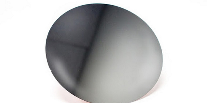
Silicon Wafer is a round disk made out of Silicon crystal used in semiconductors. They’re used in all kinds of electronic devices. It is used in semiconductors due to its stable structure.
Visit this Page for More Information: Start a Business in Computer and Electronic Product Manufacturing Industries
What are Silicon Wafers and What are they made of?
Silicon wafers are a circular disk made out of Silicon disk that is used in laptops, mobile phones, CPUs, Television. It is available in every electronic device. Silicon wafers are available in different sizes, from 1 inch silicon wafer to 11 inch silicon wafers. They are also used in Solar panels.
To make Silicon wafers, Silicon is purified, melted, and cooled to form into an ingot which is sliced and turned into discs.
Process of Making Silicon Wafers:
To make Silicon wafers, silicon is converted into ingots that are later sliced. 75% of these Silicon wafers come from Czochralski Method or CZ method.
The CZ method requires virgin polycrystalline silicon. This virgin polycrystalline silicon is placed in quartz crucible with elements from group Ⅲ and group Ⅴ called dopant.
Dopant is any impurity added in a semiconductor to modify electric conduction. The most commonly used dopants are, phosphorus, arsenic, boron, and antimony.
Related Business Plans: Electrical, Electronic Industries and Power Projects
These are divided in the P & N category.
- Forming an Ingot:
Silicon is heated to 1420℃. After polycrystalline silicon and dapants are melted into liquid a seed appears at the top of it. The crystal orientation in the seed is similar to that of the ingot. The seed and the melted silicon are rotated in opposite directions to have some uniformity.
After it is done, the seed is lifted from the liquefied silicon and rapidly pulled into shape. This rapid pulling stretches the silicon seed and reduces any defects inside it.
Then the pulling is slowed down to give the seed a little diameter. And then it is let down to cool down.
- Slicing the Ingot:
The fully grown ingot is flatten down but kept a little larger than the end product, i.e. silicon wafer.
This flatten silicon ingot is then marked to a spot to indicate its orientation. After that it is sent for inspection.
Once the inspection is done, the ingot is sent to slicing.
Due to its hardness, silicon is sliced with a diamond edged saw. It is cut a little bigger than the targeted size. This diamond edged saw minimises the damage on the silicon wafer.
Read Similar Articles: Engineering Goods Projects
- Lapping:
Lapping is the process to remove saw marks and any seeable defects in front and back of the silicon. It thins the ingot down and releases all the stress inside it from the slicing.
- Polishing:
An A grade silicon wafer goes through at least 2 or 3 stages of polishing.
The polishing has two steps.
- Stock removal
- Chemical mechanical Polishing, which is called CMP for short.
The Stock removal removes the thin layer of silicon (the stock) over the wafer. This is an important step to make sure the wafer isn’t damaged. The CMP or Chemical Mechanical polishing, gives the silicon wafer a mirror finish.
And once this is done it is packed and that’s how Silicon Wafers are made.
Read our Books Here: Books on Startup and Entrepreneurship, Business Ideas for Entrepreneurs, Startup India Stand up India, Most Profitable Small Scale Industry and Successful Business Plan for Startups
What are Silicon Wafers used for?
Silicon wafers are mainly used in integrated systems. Most of our electronic devices are made of electrical components, these components together are called “Integrated Circuit’ and Silicon Wafers are the most common semiconductor that we know of.
Here are a few uses of Silicon Wafers in more detail.
- SES/ Single Element Semiconductor:
As I mentioned before, Silicon is the most commonly found semiconductor. Due to its properties, a single Silicon can be made into wafers of size 300mm that are used in MEMS Application.
- SOI/ Silicon on Insulator:
SOI or Silicon on Insulator means to insulates a layer of monocrystalline Silicon from the wafer and this monocrystalline silicon as three applications
- Wafer bonding: in this two wafers are coated in an insulating layer then sandwich together inside a semiconductor.
- Separation by implantation of oxide or SIMOX: – It is a process in which a semiconductor wafer is blasted with oxygen ions. This is done to create a layer of buried oxide
- Smart Cut:- In it a layer of hydrogen is ingrained to specify the desired layer of semiconductor.
- Fibre Optics:
Silicon is the most cost effective IR material. If the P type and N type substrates give about 50% transmission or greater than 50%, in the wavelength of 1.5 to 6 micron, it is acceptable in IR.
Aside from that, Silicon wafers are used in Mobile phones, Television, Laptops, computers, etc. They’re also used in Tire Pressure Sensor System (TPSS).

Global Market and predictions:
The Global Market of Silicon wafers is worth $10.8 Billion as of 2020. It will likely be worth $16.01 Billion by the year 2028, with a CAGR of 5.8% between the year 2020-28.
As the tech industry gets bigger and bigger, the Silicon wafer industry will follow it, until we find a replacement for Silicon wafer Semiconductors for all our gadgets.
Biggest Competitors in the market:
- Intel Corp (INTC)
- Taiwan Semiconductor Manufacturing Co. Ltd. (TSM)
- Qualcomm Inc. (QCom)
- Broadcom Inc (AVGO)
- Texas Instrument Inc
- Micron Technology Inc
- NVIDIA Corp
- ASE Technology Holding Co. Ltd
- STMicroelectronic NV (STM)
- NXP Semiconductors NV
Biggest Competitors in Indian Market:
- Wipro
- Samsung Semiconductor
- Sankalp Semiconductor
- Applied Material.
- Masamb
- Micron Technology.
See More Links:
- Start a Business in Asia
- Start a Business in Potential Countries for Doing Business
- Best Industry for Doing Business
- Business Ideas with Low, Medium & High Investment
- Looking for Most Demandable Business Ideas for Startups
- Startup Consulting Services
- Start a Business in Africa
- Start a Business in India
- Start a Business in Middle East
- Related Videos
- Related Books
- Related Projects
- Related Market Research Reports
KBR_20Art22